HDI PCB for Image Processing
Mickael Urbino
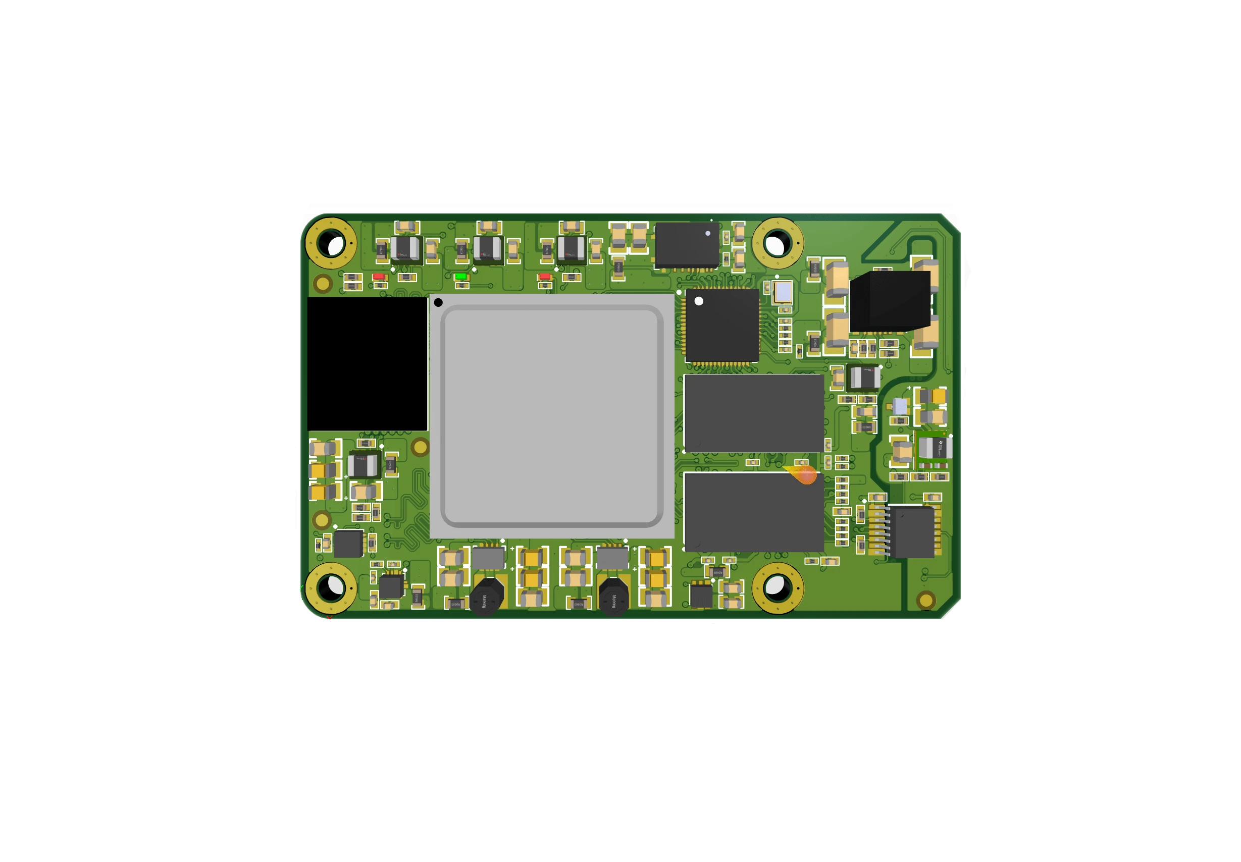
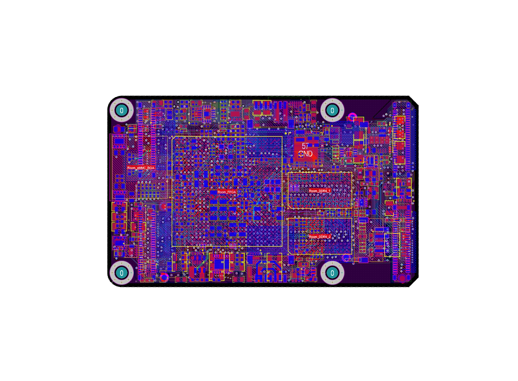
My customer was looking for someone to consolidate two of their Image Processing modules into a single PCB using Altium Designer. It resulted in this nice double-sided HDI PCB with a 70% density. (16 Layers 40mm*60mm)
The job also required the improvement of processing speed, and addition of modularity for different Image Sensors.g Speed, Add modularity for different Image Sensors.
Key Implementations:
- Upgrade from DDR3 to DDR4
- PCIe3.1 - 2.5Gb Ethernet
- Dozens of High-Speed signals
Like this project
Posted Aug 3, 2024
Consolidation of two Image Processing modules into a single PCB using Altium Designer. Here is the result. (16 Layers HDI)
Likes
1
Views
37