PCI Device - 8-Layer PCB

Adeagbo AbdulJeleel


PCI Device - 8-Layer PCB Design
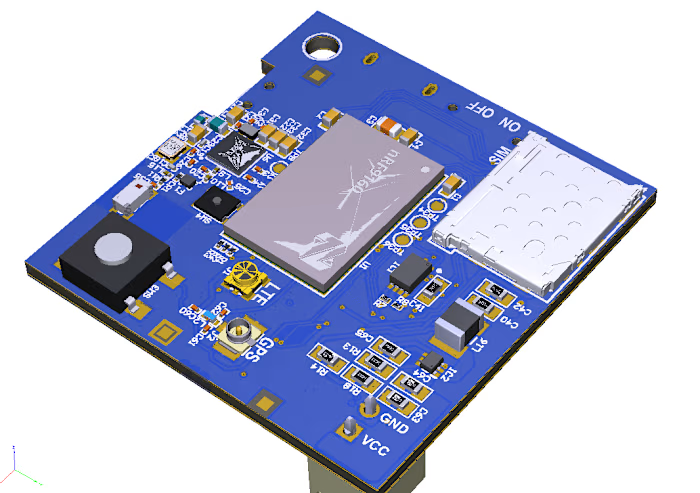
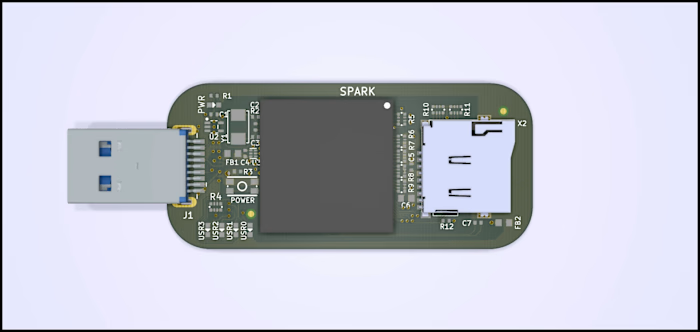
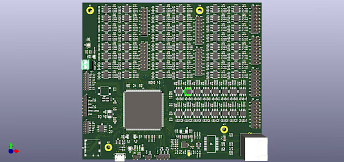
I worked on an 8-layer PCI device PCB, carrying out detailed modifications to an existing design based on the client's specific engineering requirements.
My role involved carefully reviewing the existing PCB layout, understanding the design structure and layer stack-up, and implementing the requested changes while preserving the integrity of the original design. I paid close attention to component placement, routing, power and ground distribution, layer management, and maintaining appropriate clearances throughout the board.
Working with an 8-layer PCB required careful consideration of signal routing and inter-layer connections, particularly in areas where multiple signals and components were densely packed. Each modification was implemented with attention to the existing design constraints to ensure that the updated board remained practical, reliable, and suitable for manufacturing.
This project strengthened my experience in high-layer-count PCB design, design modification, multilayer routing, and working within an established engineering design environment.
Like this project
Posted Aug 25, 2026
PCI Device - 8-Layer PCB Design I worked on an 8-layer PCI device PCB, carrying out detailed modifications to an existing design based on the client's specif...
Likes
0
Views
3