Projects using ProteusProjects using ProteusRaspberry Pi CM5 Carrier Board with Class-D Amp
In this design, Texas Instruments TPA3118 Class-D amplifier is integrated on the PCB carrying Raspberry Pi CM5. Power supply is coming from USB-PD input via Type-C port.
I/O ports
1 x HDMI
1 x DSI 22p FPC connector
2 x USB 3.0 Type-A
2 x USB 2.0 Type-A
1 x M.2 M-Key PCIe slot for SSD
1 x 3.5mm stereo Line-out jack
1 x USB Type-C Debug/Flash
1 x USB Type-C PD
1 x PWM Fan connector
1 x RGB LED 3-p connector connected to GPIO
1 x rotary encoder input connected to GPIO
ICs
Texas Instruments PCM5102A, 2.1 VRMS, 112/106/100 dB Audio Stereo DAC with PLL and 32-bit, 384 kHz PCM Interface
Texas Instruments TPA3118D2, 30-W stereo, 60-W mono, 4.5- to 26-V supply, analog input Class-D audio amplifier
Injoinic IP2721, TYPEC/PD2.0/PD3.0 Physical Layer IC for USB Type-C input Interfaces
Terminus Tech FE1.1s, USB 2.0 High Speed 4-port Hub Controller Raspberry Pi Zero Relay Board
I designed a custom Raspberry Pi Zero relay control board that combines a Raspberry Pi Zero development platform with multiple relay outputs for controlling external electrical loads.
The objective of the project was to allow the Raspberry Pi Zero to electronically control the relays, providing a practical interface between the low-voltage digital signals from the Pi and connected external devices.
My work involved developing the PCB layout around the Raspberry Pi Zero, organizing the relay circuitry, and carefully routing the control and power connections. Particular attention was given to component placement, signal routing, power distribution, isolation between the control circuitry and relay sections, and maintaining a clean, reliable board layout.
The project provided valuable experience in Raspberry Pi hardware integration, relay control, PCB design, digital interfaces, and hardware prototyping, while demonstrating how a compact embedded platform can be integrated with a dedicated control board for real-world automation applications. PWM Module - Multi-Channel PCB Design
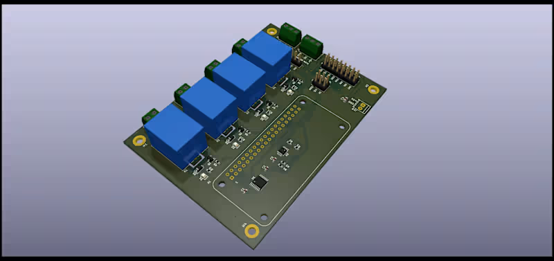
Designed a custom PCB integrating four independent PWM (Pulse Width Modulation) modules on a single board, creating a compact and practical solution for controlling multiple output channels.
The PWM modules can be used for applications such as DC motor speed control, LED brightness adjustment, and light dimming. My work involved translating the circuit requirements into a functional PCB layout, carefully arranging the four PWM sections while maintaining clear separation between functional blocks.
I focused on efficient component placement, clean signal routing, power distribution, grounding, and practical board organization. Combining four PWM channels onto a single PCB required careful planning to make effective use of the available board space while keeping the design organized and suitable for assembly.
This project strengthened my experience in multi-channel PCB design, power and signal routing, motor control applications, and practical electronics hardware development. PCI Device - 8-Layer PCB Design
I worked on an 8-layer PCI device PCB, carrying out detailed modifications to an existing design based on the client's specific engineering requirements.
My role involved carefully reviewing the existing PCB layout, understanding the design structure and layer stack-up, and implementing the requested changes while preserving the integrity of the original design. I paid close attention to component placement, routing, power and ground distribution, layer management, and maintaining appropriate clearances throughout the board.
Working with an 8-layer PCB required careful consideration of signal routing and inter-layer connections, particularly in areas where multiple signals and components were densely packed. Each modification was implemented with attention to the existing design constraints to ensure that the updated board remained practical, reliable, and suitable for manufacturing.
This project strengthened my experience in high-layer-count PCB design, design modification, multilayer routing, and working within an established engineering design environment. LTE, GPS & GSM Module PCB Design
I designed a custom PCB based on client-provided schematics and precise board dimensions, integrating LTE, GPS, and GSM communication modules into a compact and functional layout.
The project required careful component placement, routing, and consideration of the different communication and power requirements of each module. I began by reviewing the provided schematic to understand the circuit architecture, component relationships, power rails, and communication interfaces. I then organized the components according to their functional blocks and positioned critical components strategically to keep signal paths short and efficient.
A major part of the work involved routing the high-density connections while maintaining a clean and practical PCB layout. I paid close attention to power distribution, grounding, signal integrity, component spacing, and the physical board constraints provided by the client. The RF and communication sections required particularly careful routing and placement to minimize unnecessary interference and maintain reliable performance.
Although the project involved a lengthy and detailed layout process, the complexity made it a rewarding engineering challenge. It strengthened my experience in designing compact communication-focused PCBs and translating detailed schematics into a practical, manufacturable board layout.