
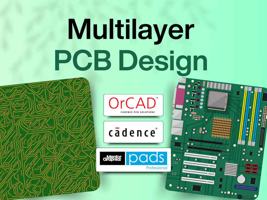
Multilayer PCB Design for High-Speed HardwareDhara Rajpura
You get high-speed, multilayer PCB designs built for real-world performance. From schematic to layout
Every step focuses on signal quality, power integrity, and clean, manufacturable output you can rely on
What's included
What I Do
I design multilayer PCBs for high-speed and embedded hardware. Every layout is built for performance, signal quality, and manufacturability
Schematic to Layout
I translate circuit logic into clean PCB layouts using controlled impedance, optimised routing, and DFM standards
High-Speed Routing
I handle BGA escape, differential pair routing, and layer stack planning for USB, DDR, PCIe, or similar high-speed signals
Power Integrity
I plan power and ground planes with via stitching and copper pours to ensure low-noise, stable power delivery
Manufacturing Files
I deliver Gerbers, BOM, drill files, and pick-and-place data ready for production — tested and IPC-compliant
Collaboration
I work directly with hardware teams and manufacturers to align on specs, tolerances, and design constraints
Contact for pricing
Tags
Altium Designer


Design Engineer
Embedded Systems Developer
Product Designer
Service provided by
Dhara Rajpura Ahmedabad, India
- 5.00
- Rating
- 2
- Followers
Multilayer PCB Design for High-Speed HardwareDhara Rajpura
Contact for pricing
Tags
Altium Designer
Design Engineer
Embedded Systems Developer
Product Designer
You get high-speed, multilayer PCB designs built for real-world performance. From schematic to layout
Every step focuses on signal quality, power integrity, and clean, manufacturable output you can rely on
What's included
What I Do
I design multilayer PCBs for high-speed and embedded hardware. Every layout is built for performance, signal quality, and manufacturability
Schematic to Layout
I translate circuit logic into clean PCB layouts using controlled impedance, optimised routing, and DFM standards
High-Speed Routing
I handle BGA escape, differential pair routing, and layer stack planning for USB, DDR, PCIe, or similar high-speed signals
Power Integrity
I plan power and ground planes with via stitching and copper pours to ensure low-noise, stable power delivery
Manufacturing Files
I deliver Gerbers, BOM, drill files, and pick-and-place data ready for production — tested and IPC-compliant
Collaboration
I work directly with hardware teams and manufacturers to align on specs, tolerances, and design constraints
Contact for pricing