
Advanced PCB DesignJhon Zumaeta
Jhon created advanced PCB designs for numerous electronic products. He ensured optimal performance and reliability through meticulous design practices.
What's included
PCB design deliverable
The client can expect at the end of a PCB design project:
Schematic Diagram: A detailed schematic showing the connections between components, including part numbers, values, and reference designators.
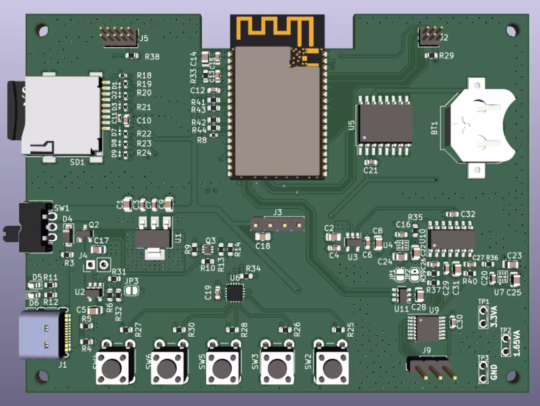
PCB Layout: The physical layout of the printed circuit board, including component placement, routing, and layers.
Gerber Files: Industry-standard files used for manufacturing the PCB, including copper layers, solder mask, silkscreen, and drill files.
Bill of Materials (BOM): A comprehensive list of all components required for assembly, along with their quantities and suppliers.
Assembly Drawings: Detailed drawings showing how components should be placed on the PCB during assembly.
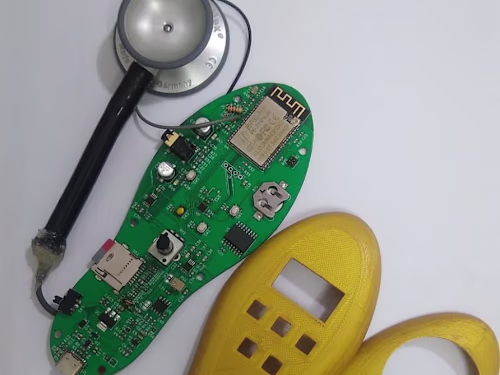
3D Models: 3D representations of the PCB and its components for mechanical integration.
Design Documentation: Any additional documentation, such as design notes, design rules, and guidelines.
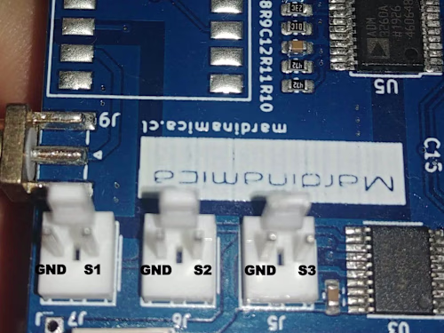
Test Points and Test Procedures: Recommendations for testing and validating the PCB design.
Design Review: A presentation or meeting to discuss the design with the client and address any questions or concerns.
Jhon's other services
Contact for pricing
Tags
Altium Designer
Embedded Systems Developer
Service provided by
Jhon Zumaeta Lima, Peru
Advanced PCB DesignJhon Zumaeta
Contact for pricing
Tags
Altium Designer
Embedded Systems Developer
Jhon created advanced PCB designs for numerous electronic products. He ensured optimal performance and reliability through meticulous design practices.
What's included
PCB design deliverable
The client can expect at the end of a PCB design project:
Schematic Diagram: A detailed schematic showing the connections between components, including part numbers, values, and reference designators.
PCB Layout: The physical layout of the printed circuit board, including component placement, routing, and layers.
Gerber Files: Industry-standard files used for manufacturing the PCB, including copper layers, solder mask, silkscreen, and drill files.
Bill of Materials (BOM): A comprehensive list of all components required for assembly, along with their quantities and suppliers.
Assembly Drawings: Detailed drawings showing how components should be placed on the PCB during assembly.
3D Models: 3D representations of the PCB and its components for mechanical integration.
Design Documentation: Any additional documentation, such as design notes, design rules, and guidelines.
Test Points and Test Procedures: Recommendations for testing and validating the PCB design.
Design Review: A presentation or meeting to discuss the design with the client and address any questions or concerns.
Jhon's other services
Contact for pricing