
If your PCB works but the product still has no body, this is the step that gets you to something a manufacturer can actually price.
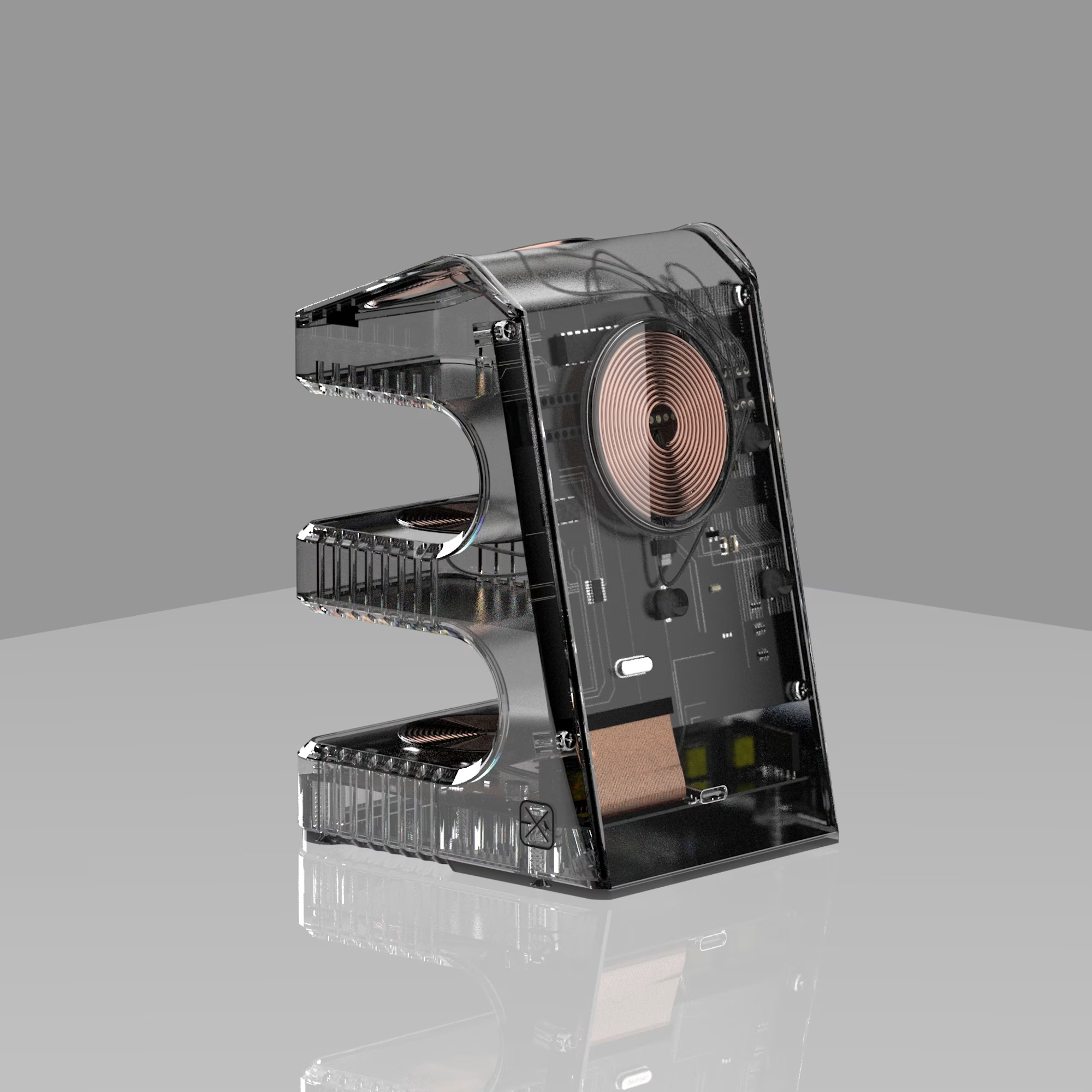
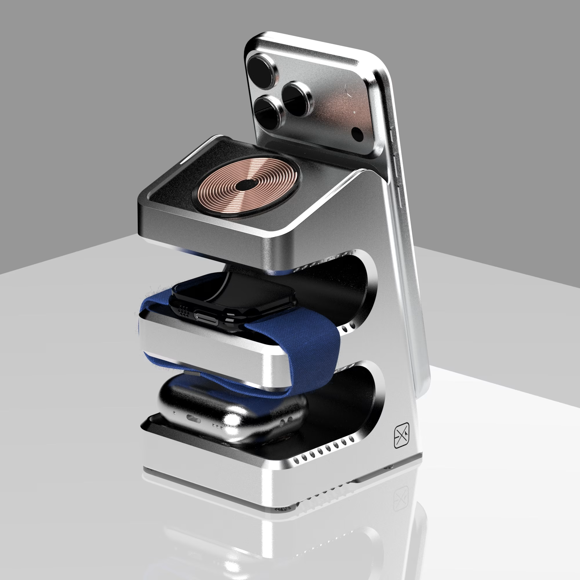
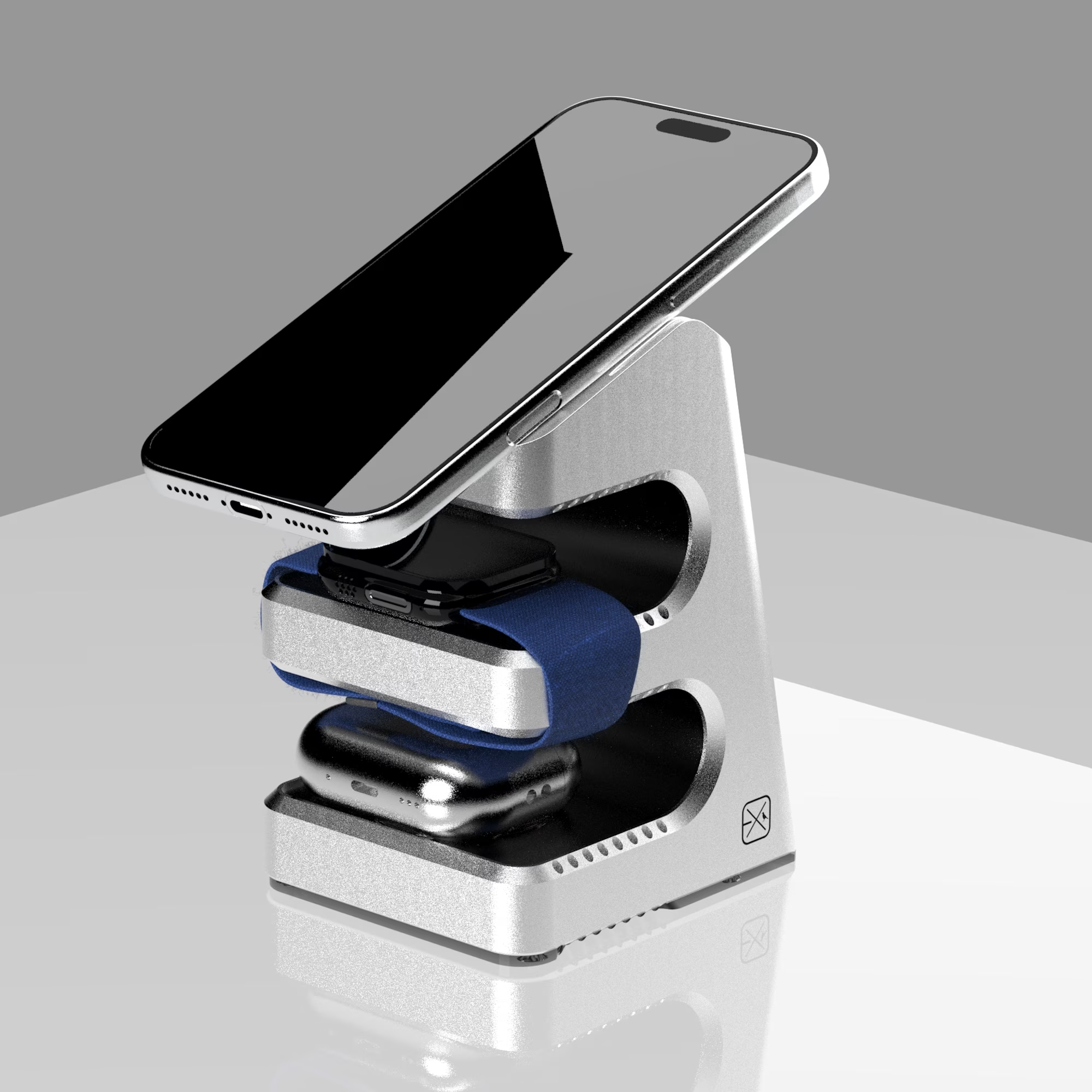
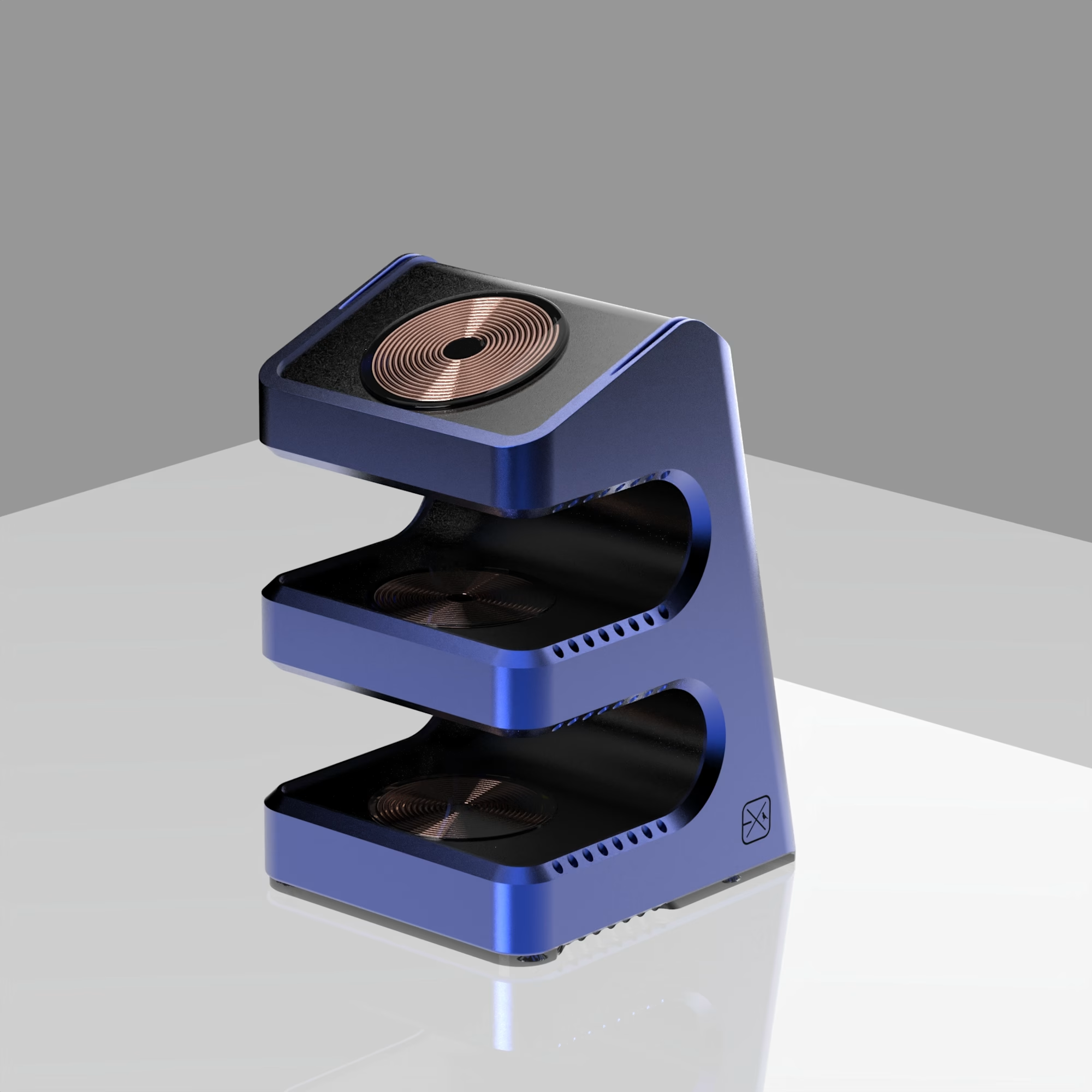
I design the enclosure around your existing electronics — the housing, the internal architecture, how the board and connectors sit inside it, and how it gets made at volume. Not a render of an idea. A design with wall thickness, draft, an assembly method, and a process behind it.
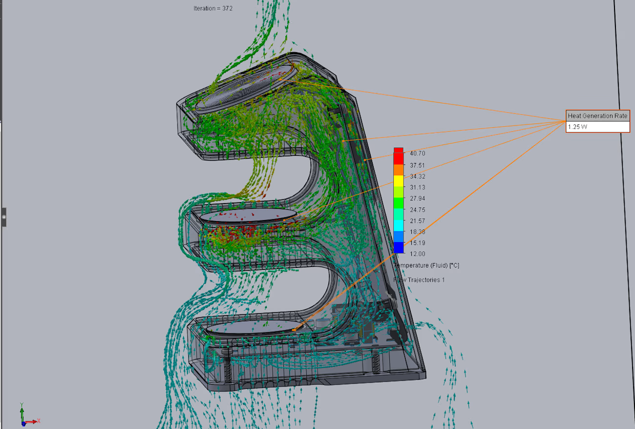
I check the things that get expensive later: clearance conflicts, undercut faces that force side actions in the tool, wall sections that sink or warp, heat with nowhere to go. Catching those on a model costs nothing. Catching them after steel is cut costs a tool.
Every tier ends at a usable point — a decided direction, a CAD file, or a package a factory can quote from.
What I don't do: PCB layout, circuit design, or firmware. Mold and tooling engineering is executed by a tooling specialist. I write the spec that engineer works from and stay in the loop through tool release.
Bring me a board outline, component datasheets, and a rough sense of volume, and I'll tell you what's realistic before you commit.
Get it for$750.00
Concept Architecture
$750.00
2 form factor directions, one refined, with CAD and layout rationale.
Tags
KeyShot

SolidWorks

Product Design Consultant
Consumer Electronics
Design for Manufacturing
Enclosure Design
Product created by
Eugenio Cruz Cornejo Argentina
- $5k+
- Earned
- 5
- Paid projects
- 5.00
- Rating
- 13
- Followers
Get it for$750.00
Concept Architecture
$750.00
2 form factor directions, one refined, with CAD and layout rationale.
Tags
KeyShot
SolidWorks
Product Design Consultant
Consumer Electronics
Design for Manufacturing
Enclosure Design
If your PCB works but the product still has no body, this is the step that gets you to something a manufacturer can actually price.
I design the enclosure around your existing electronics — the housing, the internal architecture, how the board and connectors sit inside it, and how it gets made at volume. Not a render of an idea. A design with wall thickness, draft, an assembly method, and a process behind it.
I check the things that get expensive later: clearance conflicts, undercut faces that force side actions in the tool, wall sections that sink or warp, heat with nowhere to go. Catching those on a model costs nothing. Catching them after steel is cut costs a tool.
Every tier ends at a usable point — a decided direction, a CAD file, or a package a factory can quote from.
What I don't do: PCB layout, circuit design, or firmware. Mold and tooling engineering is executed by a tooling specialist. I write the spec that engineer works from and stay in the loop through tool release.
Bring me a board outline, component datasheets, and a rough sense of volume, and I'll tell you what's realistic before you commit.
$750.00